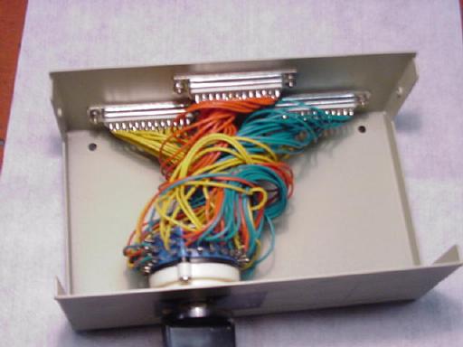
Manual parallel port switch boxes make good homes for projects which use the parallel port. You should purchase a box that has all leads passing through from the common to switched ports. Try to find a metal box which uses point to point wiring, (no printed circuit board).

The unmodified printer box with cover removed appears above. Looks pretty scary but there is plenty of room for the circuit inside and carefully labeling the wires you use will help you keep track of things. The first step is to remove the screws of one of the switched output port connectors. Here I used port A.
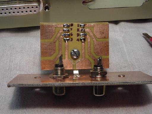
I elected to use half of a small RadioShack ™ proto-board for construction. The bottom of the board is shown here. An 8 pin dip socket is mounted on the other side. I have found it useful to label the pins to avoid the confusion caused my the mirror image you get when viewing the chip from the bottom. A small bracket made from a solder lug supports the board on a scrap piece of PC board. The PC board was first placed into the switch box and the hole outline and screw slots from the vacated D connector were traced onto the board. Then screw holes and holes for the RCA phono jacks which will eventually pass power and the analog signal to the ADC were drilled through the PC board. Despite the way the picture looks the RCA connectors are not touching any part of the proto-board.
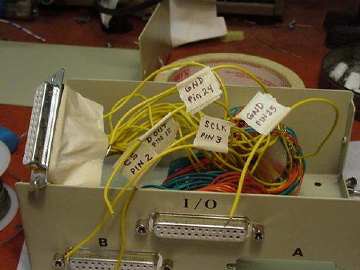
Wires 2, 3, 12, 24, and 25 were then unsoldered and labeled one at a time from the 25 pin D connector which was once port A. I just used masking tape. I also placed some tape around the back of the D connector since it would be lying loose in the box for the remainder of its life.
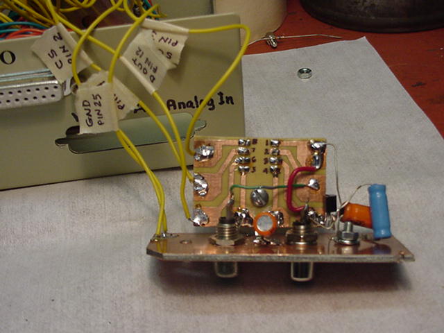
Now comes the wiring and placement of parts. Since the PC board scrap is the ground plane for the project you can solder anything that goes to ground directly to it. Don't forget to run a lead from the pad for the MAX187 pin 5 to ground. There are so few parts that you should have little trouble making everything fit. Test to make sure that the mounting screws won't contact anything they shouldn't.
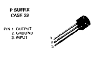 This is the pin out for the T78L05
voltage regulator IC. The MAX 187 IC follows the standard DIP package
convention. Looking down on the chip from above, the end with the notch
indicates pins 1 and 8 with pin 1 on the left.
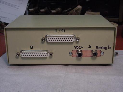
When mounted in the box it looks like this from behind. Be sure to label the jacks before you put the lid on and forget which is which.
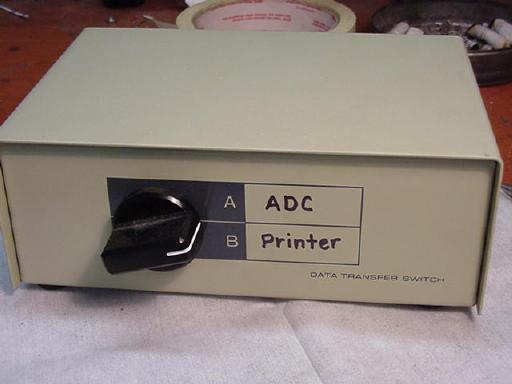
Here's the front view.
There are lots of other ways you mount and wire this project up. Wire length, with the exception of the ground connections isn't very critical in this project so you could have used a less cramped approach. Feel free to modify it anyway you wish, so long as it works. Some people would object to the use of RCA type phono jacks. Use something else if you wish. This is a good first project simply because it is so non-critical.
Related Links:
All material including photos on this page ©2000 by Radio-Sky Publishing
4/30/2000
HOME | BEGINNERS | JUPITER | SOLAR | PULSARS | PROJECTS | FAQ | BOOKS | SOFTWARE | SUPPORT | ORDERING | LINKS